


 购买咨询热线/Phone:
 邮箱/Email:
 地址:
地址:Description
0100-71267 电容式刻蚀机已达到国际先进水平的7纳米和5纳米
半导体制造设备是指用于制造和测试半导体芯片的设备,0100-71267主要有三大核心设备,分别是刻蚀设备、薄膜沉积设备和光刻设备。
刻蚀设备占比30%,薄膜沉积设备占比25%,光刻设备占比23%,这三大设备占了整个设备投资额的约80%。
在刻蚀设备方面,电容式刻蚀机已达到国际先进水平的7纳米和5纳米;北方华创属于平台型公司,基本上所有的设备都有。
在薄膜沉积设备方面,物理气相沉积做的较好的是北方华创;化学气相沉积做的较好的是拓荆科技;原子层沉积做的较好的是微导纳米。
此外,检测设备也属于半导体制造设备,不同于测试设备,检测设备是从头到尾的每一个环节都会涉及到的缺陷检测。而测试设备是指做好之后的封装和测试。在检测设备方面,精测电子和赛腾股份在面板检测或消费电子检测方面表现较好。
半导体制造设备是指在半导体制造过程中使用的各种设备,0100-71267用于生产半导体器件和集成电路。这些设备种类繁多,包括但不限于以下几类:
清洗设备:用于清洗半导体材料表面,去除杂质和污染物,保证材料的纯净度和表面的清洁度。
热处理设备:用于对半导体材料进行加热和冷却处理,实现材料的掺杂、氧化、还原等工艺操作。
光刻设备:用于将设计好的电路图案转移到半导体材料表面上的光刻胶上,是制造集成电路的关键设备之一。
刻蚀设备:用于对半导体材料进行刻蚀,将光刻胶上的电路图案转移到材料上,形成电路和器件的结构。
离子注入设备:用于将离子注入到半导体材料中,实现材料的掺杂和改性,形成不同的导电类型和器件特性。
化学气相沉积设备:用于在半导体材料表面形成各种薄膜,如氧化层、氮化层、多晶硅层等。
物理气相沉积设备:用于在半导体材料表面形成金属、合金等材料,形成电路和器件的连接和导电。
封装设备:用于将制造好的集成电路进行封装和测试,保证其可靠性和稳定性。
这些设备在半导体制造过程中起着至关重要的作用,0100-71267是实现半导体器件和集成电路生产的关键环节。随着技术的发展和进步,半导体制造设备也在不断更新和升级,提高生产效率和制造精度,为半导体产业的发展提供有力支持。
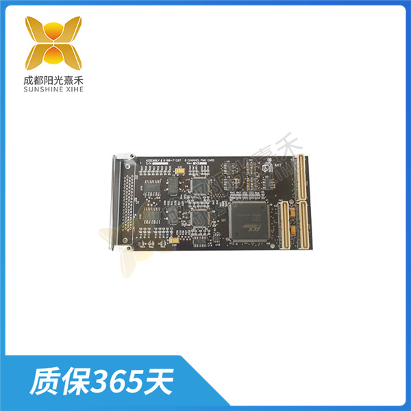
0100-71267 电容式刻蚀机已达到国际先进水平的7纳米和5纳米
Semiconductor manufacturing equipment refers to the equipment used to manufacture and test semiconductor chips, 0100-71267 mainly has three core equipment, respectively, etching equipment, thin film deposition equipment and lithography equipment.
Etching equipment accounted for 30%, film deposition equipment accounted for 25%, lithography equipment accounted for 23%, and these three equipment accounted for about 80% of the entire equipment investment.
In terms of etching equipment, capacitive etching machine has reached the international advanced level of 7 nm and 5 nm; Naura is a platform company and basically has all the equipment.
In terms of film deposition equipment, the best physical vapor deposition is NAURA; The best chemical vapor deposition is Tuojing Technology; Atomic layer deposition is better done by microadmittance meters.
In addition, the detection equipment is also a semiconductor manufacturing equipment, which is different from the test equipment, and the detection equipment is the defect detection involved in every link from the beginning to the end. The test equipment refers to the packaging and testing after it is done. In terms of testing equipment, precision testing Electronics and Seteng shares perform better in panel testing or consumer electronics testing.
Semiconductor manufacturing equipment refers to various devices used in the semiconductor manufacturing process, and 0100-71267 is used to produce semiconductor devices and integrated circuits. These devices come in a wide variety, including but not limited to the following categories:
Cleaning equipment: used to clean the surface of semiconductor materials, remove impurities and pollutants, and ensure the purity of the material and the cleanliness of the surface.
Heat treatment equipment: used for heating and cooling semiconductor materials to achieve doping, oxidation, reduction and other process operations.
Lithography equipment: used to transfer the designed circuit pattern to the photoresist on the surface of the semiconductor material, is one of the key equipment for manufacturing integrated circuits.
Etching equipment: used to etch semiconductor materials, transfer the circuit pattern on the photoresist to the material, forming the structure of the circuit and device.
Ion implantation equipment: used to inject ions into semiconductor materials to achieve doping and modification of materials to form different conductive types and device characteristics.
Chemical vapor deposition equipment: used to form various thin films on the surface of semiconductor materials, such as oxide layer, nitriding layer, polysilicon layer, etc.
Physical vapor deposition equipment: used to form metals, alloys and other materials on the surface of semiconductor materials to form the connection and conduction of circuits and devices.
Packaging equipment: used to package and test the manufactured integrated circuit to ensure its reliability and stability.
These devices play a vital role in the semiconductor manufacturing process, and 0100-71267 is a key link in the production of semiconductor devices and integrated circuits. With the development and progress of technology, semiconductor manufacturing equipment is also constantly updated and upgraded to improve production efficiency and manufacturing accuracy, providing strong support for the development of the semiconductor industry.
 购买咨询热线/Phone:18859254943
- 邮箱/Email:sales@ygdcs.com
- 地址:成都高新区天益街北巷52号附14号2层


