


 购买咨询热线/Phone:
 邮箱/Email:
 地址:
地址:Description
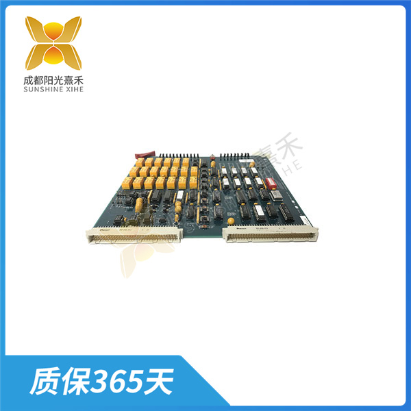
810-370141-001 可以用玻璃、陶瓷、硅等材料制成
大面积多层集成电路模块是一种高度集成的电子器件,810-370141-001包含了多个电子元器件(如晶体管、电阻器、电容器等)在一个较小的基板上。这些元器件通过电路互连,实现特定的电子功能。由于其高集成度,大面积多层集成电路模块广泛应用于各种领域,如通信、计算机、医疗设备等。
在制造大面积多层集成电路模块时,通常需要经过以下几个步骤:
基板制作:首先需要制作一个薄片状的基板,810-370141-001可以用玻璃、陶瓷、硅等材料制成。基板通常具有平坦和光滑的表面,以便在其上形成集成电路。
薄膜制备:在基板上制备一层或多层薄膜,这些薄膜是集成电路的主要组成部分。薄膜的厚度和成分可以根据需要进行调整,以满足电路的性能要求。
电路制作:通过光刻、刻蚀、镀膜等工艺,在薄膜上形成电路互连。这一步需要精确控制工艺参数,以确保电路的精度和可靠性。
元件制作:在薄膜上制作各种电子元件,如晶体管、电阻器、电容器等。这些元件通常是通过沉积、刻蚀、光刻等技术制成的。
封装测试:将制作好的集成电路模块进行封装,并对其进行测试。测试内容包括功能测试、性能测试和可靠性测试等。
大面积多层集成电路模块的应用范围非常广泛,例如通信领域中的手机、无线通信基站、路由器等;计算机领域中的中央处理器(CPU)、图形处理器(GPU)、存储器等;医疗设备中的心电图机、超声波设备等;以及军事领域中的雷达、导航系统等。随着科技的不断进步,大面积多层集成电路模块的应用前景将会越来越广泛。
大面积多层集成电路模块是一种集成电路封装形式,它将多个集成电路芯片堆叠在一起,并通过金属导线连接,形成一个高度集成的模块。这种封装形式可以提高集成电路的集成度和性能,同时减小电路的体积和重量。
大面积多层集成电路模块通常由多层电路板、芯片、金属导线和封装材料组成。电路板上的金属导线将芯片连接在一起,形成电路。封装材料通常是塑料或陶瓷,用于保护芯片和电路板。
大面积多层集成电路模块广泛应用于计算机、通信、消费电子等领域。它具有高集成度、高性能、小体积、低成本等优点,可以满足不同应用场景的需求。
810-370141-001 可以用玻璃、陶瓷、硅等材料制成
A large area multilayer integrated circuit module is a highly integrated electronic device, 810-370141-001 contains multiple electronic components (such as transistors, resistors, capacitors, etc.) on a smaller substrate. These components are interconnected through circuits to perform specific electronic functions. Due to its high integration, large area multilayer integrated circuit modules are widely used in various fields, such as communications, computers, medical equipment and so on.
When manufacturing a large area multilayer integrated circuit module, it is usually necessary to go through the following steps:
Substrate production: First need to make a thin sheet substrate, 810-370141-001 can be made of glass, ceramics, silicon and other materials. The substrate usually has a flat and smooth surface so that integrated circuits can be formed on it.
Film preparation: The preparation of one or more layers of films on the substrate, these films are the main components of the integrated circuit. The thickness and composition of the film can be adjusted as needed to meet the performance requirements of the circuit.
Circuit production: Through lithography, etching, coating and other processes, circuit interconnection is formed on the film. This step requires precise control of process parameters to ensure the accuracy and reliability of the circuit.
Component production: The production of various electronic components on the film, such as transistors, resistors, capacitors, etc. These elements are usually made by deposition, etching, lithography and other techniques.
Package and test: The made integrated circuit module is packaged and tested. The test contents include functional test, performance test and reliability test.
The application range of large-area multilayer integrated circuit modules is very wide, such as mobile phones, wireless communication base stations, routers, etc. Central processing unit (CPU), graphics processing unit (GPU), memory, etc.; Electrocardiograph and ultrasonic equipment in medical equipment; As well as radar and navigation systems in the military field. With the continuous progress of science and technology, the application prospect of large-area multilayer integrated circuit modules will be more and more extensive.
A large-area multilayer integrated circuit module is a form of integrated circuit packaging that stacks multiple integrated circuit chips together and connects them through metal wires to form a highly integrated module. This form of packaging can improve the integration and performance of integrated circuits, while reducing the size and weight of the circuit.
The large-area multilayer integrated circuit module is usually composed of multilayer circuit board, chip, metal wire and packaging material. Metal wires on the circuit board connect the chips together to form the circuit. The packaging material is usually plastic or ceramic and is used to protect chips and circuit boards.
Large area multilayer integrated circuit modules are widely used in computer, communication, consumer electronics and other fields. It has the advantages of high integration, high performance, small size and low cost, and can meet the needs of different application scenarios.
 购买咨询热线/Phone:18859254943
- 邮箱/Email:sales@ygdcs.com
- 地址:成都高新区天益街北巷52号附14号2层


