")
")
 购买咨询热线/Phone:
 邮箱/Email:
 地址:
地址:Description
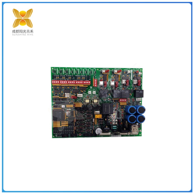
IS200TDBSH6ABB 可以轻松地设计复杂的电路布局
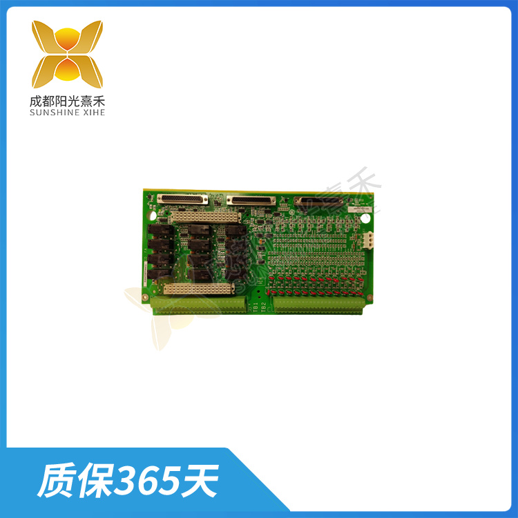
印刷电路板(Printed Circuit Board,PCB)是一种用于电子组件连接的基板,通常是由绝缘材料制成,如酚醛树脂或环氧树脂。在PCB上,导电路径被印刷或蚀刻出来,以连接各种电子组件。这些路径被称为导线或轨迹,并且通常由铜制成。
印刷电路板IS200TDBSH6ABB的主要优点包括:
高可靠性:由于电子组件之间的连接是通过PCB上的固定路径进行的,因此减少了因手动焊接或连接不良导致的故障。
易于维护:如果某个组件出现故障,可以很容易地将其从PCB上取下并更换,而无需更改其他组件的连接。
易于制造:使用自动化生产线,可以大规模、高效地生产PCB。
小型化:PCB允许将多个组件紧密地组合在一起,从而实现设备的小型化。
易于设计:使用电子设计自动化(EDA)工具,可以轻松地设计复杂的电路布局。
PCB的制造过程通常包括以下几个步骤:
设计:使用CAD(计算机辅助设计)软件创建电路板的布局和布线。
制造:将设计数据发送到制造厂,在那里使用光刻技术将电路图案转移到敷铜板上。
蚀刻:使用化学蚀刻剂去除未被光刻胶保护的铜层,形成电路图案。
钻孔:在PCB上钻孔,以便安装电子组件和连接内层电路(对于多层板)。
表面处理:可能需要对裸露的铜表面进行处理,如涂覆阻焊层或焊接掩模。
组装:将电子组件焊接到PCB上,并进行必要的测试。
最终测试:测试组装好的PCB以确保其按设计要求工作。
PCB广泛应用于各种电子设备中,如计算机、手机、医疗设备、汽车控制系统等。随着技术的进步,PCB的设计和制造过程也在不断发展和改进,以满足更复杂电路和更高性能的需求。
IS200TDBSH6ABB 可以轻松地设计复杂的电路布局
A Printed Circuit Board (PCB) is a substrate used to connect electronic components, usually made of an insulating material such as phenolic resin or epoxy resin. On the PCB, conductive paths are printed or etched out to connect various electronic components. These paths are called wires or tracks, and are usually made of copper.
Key benefits of the IS200TDBSH6ABB Printed Circuit Board include:
High reliability: Because the connection between the electronic components is made through a fixed path on the PCB, the failure caused by manual welding or poor connection is reduced.
Easy maintenance: If a component fails, it can be easily removed from the PCB and replaced without changing the connections of other components.
Easy to manufacture: Using automated production lines, PCBS can be produced on a large scale and efficiently.
Miniaturization: PCBS allow multiple components to be tightly grouped together, enabling the miniaturization of the device.
Ease of design: Using Electronic Design Automation (EDA) tools, it is easy to design complex circuit layouts.
The manufacturing process of a PCB usually includes the following steps:
Design: Use CAD (Computer Aided Design) software to create the layout and wiring of the circuit board.
Fabrication: The design data is sent to the manufacturing plant, where the circuit pattern is transferred to the copper-coated plate using lithography.
Etching: A chemical etching agent is used to remove the copper layer that is not protected by the photoresist to form a circuit pattern.
Drilling: Drilling holes in the PCB to install the electronic components and connect the inner circuit (for multilayer boards).
Surface treatment: Exposed copper surfaces may need to be treated, such as applying a solder mask or welding mask.
Assembly: Solder the electronic components to the PCB and perform the necessary tests.
Final test: Test the assembled PCB to ensure that it works as designed.
PCB is widely used in a variety of electronic equipment, such as computers, mobile phones, medical equipment, automotive control systems and so on. As technology advances, PCB design and manufacturing processes are also evolving and improving to meet the needs of more complex circuits and higher performance.
| sr469 – p1 – hi – a20 – ege469电机管理继电器 | G408-0001 ULTRA SLIMPAK®直流供电直流输入场可配置隔离器 |
| 8202-HO-IS GE 8通道是AO, 4-20 mA与哈特 | VMIACC-0584 GE CompactPCI®单板计算机 |
| SR469继电器 | ADTRON模拟输入模块 |
| XPSMC32ZP施耐德安全控制器 | RMP200-8远程多用途输入输出康士伯 |
| DDC779BE102 3BHE006805R0002以太网控制模块ABB | ACC-24E2轴扩展板Delta Tau |
| NI-9263 NI C系列电压输出模块 | UAC389AE02 ABB模拟输入模块 |
| YOKOGAWA程序控制器UP55A | ADTRON模拟输入模块 |
| 8201-HI-IS GE 8通道IS AI, 4-20mA带Hart | CB6687-2L PILLAR模拟输入模块 |
| TCSESM043F2CS0 Schneider以太网TCP/IP管理交换机 | SPAU140C ABB同步检查继电器 |
| 1336F-BRF50-AA-EN-HAS2艾伦-布拉德利可调频率驱动器制造 | 横河控制系统ANB10D-420/CU2N/NDEL |
| 1336-BDB-SP11C Allen-Bradley栅极驱动器PCB制造 | 192061B-02多功能电缆NI |
| SR469-P5-HI-A20-H GE电机管理继电器 | 太平洋科学步进驱动器 |
| 140NRP31200C Schneider以太网光纤转换器 | 霍尼韦尔单通道控制卡催化 |
| TC-PPD011 Honeywell电池扩展模块 | 霍尼韦尔单通道控制卡催化 |
| TK-FPDXX2霍尼韦尔电池扩展模块 | 步进电机太平洋科学公司 |
| 369-HI-0-M-F-E-0 GE电机管理继电器 | TS2640N321E64 TAMAGAWA无刷变压器 |
| PPD513 A24-110110静态励磁系统ABB | 05704-A-0122 HONEYWELL高性能压力传感器 |
 购买咨询热线/Phone:18859254943
- 邮箱/Email:sales@ygdcs.com
- 地址:成都高新区天益街北巷52号附14号2层