购买咨询热线/Phone:
 邮箱/Email:
 地址:
地址:Description
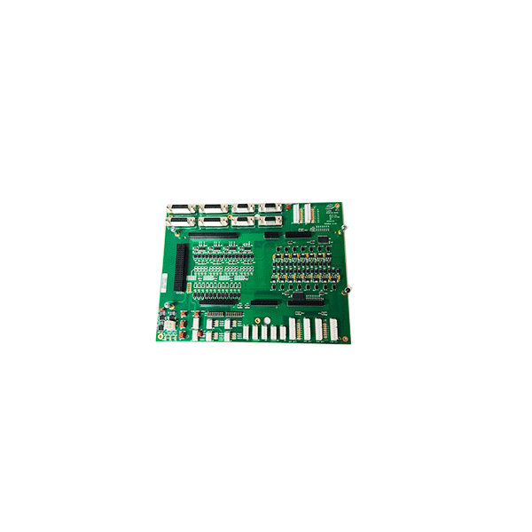
P30B04010PCKST 广泛使用在模拟电路与数字电路的场效晶体管
MOSFET(Metal Oxide Semiconductor Field Effect Transistor,金属氧化物半导体场效应晶体管)是一种功率晶体管,P30B04010PCKST
利用电压来控制电流,具有驱动功率小、开关速度高、无二次击穿、安全工作区宽等特点。
MOSFET的工作原理是通过改变加在栅极和源极之间的电压,改变半导体内部的电场分布,从而控制源极和漏极之间的电流。当栅极和源极之间的电压足够高时,半导体内部的电场变得足够强,使得源极和漏极之间的通道开启,电流得以通过。
MOSFET具有许多优点,例如高输入阻抗、低功耗、低噪声等。同时,它也有一些缺点,例如耐压低、电流小等。因此,在实际应用中,P30B04010PCKST
需要根据具体需求选择适合的MOSFET型号和参数。
MOSFET 功率晶体管全称为金属-氧化物半导体场效应晶体管,是一种广泛使用在模拟电路与数字电路的场效晶体管。按工作载流子的极性不同可分为“N 型(增强型)”与“P 型(耗尽型)”两种。以 N 型(增强型)为例,其剖面图如下:
MOSFET 功率晶体管的漏-源之间有一个 PN 结,用绿色的“+”和红色的“-”分别代表空穴和电子。电子从源极流向漏极,但源极和漏极中间还有一个阻碍就是 P 型硅半导体材料其中有大量带正电的空穴。此时漏极 D 与衬底之间的 PN 结处于反向,因此漏-源之间不能导电。
如果在栅极 G 与源极 S 之间加一电压 V,此时栅极与衬底可看作电容器的两个极板,绝缘层和栅极的界面上感应出正电和绝缘层和 P 型栅极界面上感应出负电荷。这个负电荷与衬底的多子极性相反,称为反型层。有可能将漏-源连接形成导电沟道,则产生正向工作电流 I。如果改变电压 V 即可控制工作电流 I,并呈较好的线性关系。

P30B04010PCKST 广泛使用在模拟电路与数字电路的场效晶体管
A Metal Oxide Semiconductor Field Effect Transistor (MOSFET) is a power transistor, P30B04010PCKST
Using voltage to control the current has the characteristics of small driving power, high switching speed, no secondary breakdown, wide safe working area and so on.
Mosfets work by changing the electric field distribution inside the semiconductor by changing the voltage applied between the gate and the source, thereby controlling the current between the source and drain. When the voltage between the gate and the source is high enough, the electric field inside the semiconductor becomes strong enough for the channel between the source and drain to open and the current to pass through.
Mosfets have many advantages, such as high input impedance, low power consumption, and low noise. At the same time, it also has some disadvantages, such as low voltage, low current and so on. Therefore, in practical applications, P30B04010PCKST
Select an appropriate MOSFET model and parameters based on your requirements.
MOSFET power transistor, full name of metal-oxide semiconductor field effect transistor, is a kind of field effect transistor widely used in analog circuits and digital circuits. According to the polarity of the working carrier can be divided into “N type (enhanced type)” and “P type (depletion type)” two. Taking type N (enhanced) as an example, its profile is as follows:
The MOSFET power transistor has a PN junction between the leak-source, with a green “+” and a red “-” representing holes and electrons, respectively. Electrons flow from the source to the drain, but there is a barrier between the source and drain that P-type silicon semiconductor materials have a large number of positively charged holes. At this time, the PN junction between the drain D and the substrate is in reverse, so the drain-source cannot conduct electricity.
If a voltage V is added between the gate G and the source S, then the gate and the substrate can be regarded as two plates of the capacitor, and positive charges are induced on the interface of the insulation layer and the gate, and negative charges are induced on the interface of the insulation layer and the P-type gate. This negative charge is opposite to the polarity of the polyons of the substrate and is called the antitype layer. It is possible to connect the drain-source to form a conductive channel, which generates a forward operating current I. If the voltage V is changed, the working current I can be controlled, and the linear relationship is better.

 购买咨询热线/Phone:18859254943
- 邮箱/Email:sales@ygdcs.com
- 地址:成都高新区天益街北巷52号附14号2层